
Features
1. Continuing Adjustment of Field of View
2. High Depth of Field, Lens Parfocalization
3. Central Position and Definition Remain Unchanged (Parfocalization), When Continuing Adjust Zoom Multiple.
4. Super Long Working Distance of 30mm
5. With Modular Structure and Flexible Expansibility
Applications
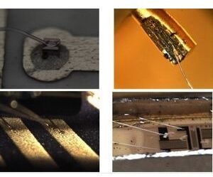
1. Widely Used for the Inspection of Micro-structure of Large Silicon Chip
2. Analysis of Bare IC Structure and the Inspection of Defective Sample
3. ITO Clearance of LCD Module and COG Observation
4. Observation and Analysis of Metallographic Structure
5. Micro-observation of Reflective Material
6. Optional 2D/3D Manual Viewer to Inspect SMT Solder Bead

Specifications
Zoom Range | 0.3X—2.2X |
Zoom Ratio | 1:7 |
Coaxial Device | 3X Objective Lens |
Coupler | 1X |
Spot Light | 3W, Brightness Adjustable, Power Supply: AC90-240V, Output Voltage: DC 12V/0.5A |
Minimum Resolution | 1μm |
Total Magnification | 3X-600X (17”Display, 1/3”CCD) |
Working Distance | 30mm |
C-mount | 1X C-mount Interface |
White Post Stand | Coarse/FineTuning with Scale Unit is 2μm |
Optical Parameters
Model | HDM-600 |
N.A. | 0.025−0.118 |
Res.(lp/mm) | 75−352 |
MAG. | 1.05X−7.35X |
D.O.F.(mm) | 0.88−0.04 |
W.D.(mm) | 30 |
F.O.V.(mm)1/2" | 7.6−1.1 |